Donor and acceptor characteristics of native point defects in GaN
Abstract
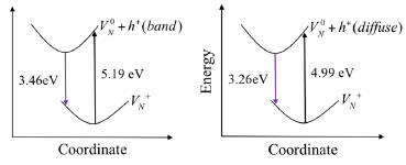
The semiconducting behaviour and optoelectronic response of gallium nitride is governed by point defect processes, which, despite many years of research, remain poorly understood. The key difficulty in the description of the dominant charged defects is determining a consistent position of the corresponding defect levels, which is difficult to derive using standard supercell calculations. In a complementary approach, we take advantage of the embedded cluster methodology that provides direct access to a common zero of the electrostatic potential for all point defects in all charge states. Charged defects polarise a host dielectric material with long-range forces that strongly affect the outcome of defect simulations; to account for the polarisation, we couple embedding with the hybrid quantum mechanical/molecular mechanical approach and investigate the structure, formation and ionisation energies, and equilibrium concentrations of native point defects in wurtzite GaN at a chemically accurate hybrid-density-functional-theory level. N vacancies are the most thermodynamically favourable native defects in GaN, which contribute to the n-type character of as-grown GaN but are not the main source, a result that is consistent with experiment. Our calculations show no native point defects can form thermodynamically stable acceptor states. GaN can be easily doped n-type, but, in equilibrium conditions at moderate temperatures acceptor dopants will be compensated by N vacancies and no significant hole concentrations will be observed, indicating non-equilibrium processes must dominate in p-type GaN. We identify spectroscopic signatures of native defects in the infrared, visible and ultraviolet luminescence ranges and complementary spectroscopies. Crucially, we calculate the effective-mass-like-state levels associated with electrons and holes bound in diffuse orbitals. These levels may be accessible in competition with more strongly-localised states in luminescence processes and allow the attribution of the observed 3.46 and 3.27 eV UV peaks in a broad range of GaN samples to the presence of N vacancies.
Hmm, what to say about this paper. First of all, a lot of really good work by Zijuan. There is a lot of information here which should be useful for experimentalists in the field. We were met with a lot of criticism for this work, mainly it seems because people in the field doing electronic structure calculations were not familiar with the method. The results, however, when using hybrid functionals similar to those used by others who performed plane-wave DFT calculations, agree reasonably well with other studies. The BB1k functional, which is very rarely used in solid-state studies, provides some intriguing results for the optical absorption and emission properties of defects in GaN.
John Buckeridge
Lecturer in Energy Engineering and Materials Devices
Materials physicist working at the School of Engineering - Division of Electrical and Electronic Engineering, London South Bank University.